| Board design know-how for switching power supplies with low noise and stable operation. |
| File name:PCB-design-manual.pdf |
| ・PCB creepage distance |
| ・Basic rules for power supply PCB board design |
| ・Primary side main parts placement and pattern |
| ・Secondary side main parts placement and pattern |
| ・Copper through-hole VIAs in switching current roop |
| ・Primary Clamp Circuit |
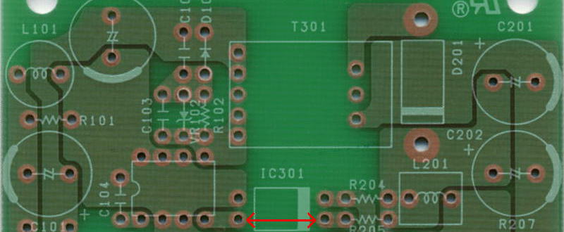
| ・Capacitor near main IC |
| ・Output voltage detection circuit |
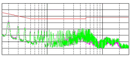
| Conduction noise in the Average PCB Design |
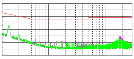
Conduction noise in the Best PCB Design |
 |
 |